Author Affiliations
Abstract
1 College of Physics, MIIT Key Laboratory of Aerospace Information Materials and Physics, Key Laboratory for Intelligent Nano Materials and Devices, Nanjing University of Aeronautics and Astronautics, Nanjing 211106, China
2 e-mail: cxkan@nuaa.edu.cn
Low-power, flexible, and integrated photodetectors have attracted increasing attention due to their potential applications of photosensing, astronomy, communications, wearable electronics, etc. Herein, the samples of ZnO microwires having -type (Sb-doped ZnO, ZnO:Sb) and -type (Ga-doped ZnO, ZnO:Ga) conduction properties were synthesized individually. Sequentially, a homojunction vertical structure photodiode involving a single ZnO:Sb microwire crossed with a ZnO:Ga microwire, which can detect ultraviolet light signals, was constructed. When exposed under 360 nm light illumination at , the proposed photodiode reveals pronounced photodetection features, including a largest on/off ratio of , responsivity of 2.3 A/W, specific detectivity of Jones, noise equivalent power of , and superior photoelectron conversion efficiency of . The photodiode also exhibits a fast response/recovery time of 0.48 ms/9.41 ms. Further, we propose a facile and scalable construction scheme to integrate a microwires homojunction component into a flexible, array-type detector, which manifests significant flexibility and electrical stability with insignificant degradation. Moreover, the as-constructed array unit can be integrated into a practical photoimaging system, which demonstrates remarkable high-resolution single-pixel imaging capability. The results represented in this work may supply a workable approach for developing low-dimensional ZnO-based homojunction optoelectronic devices with low-consumption, flexible, and integrated characteristics.
Photonics Research
2024, 12(4): 648

Author Affiliations
Abstract
1 College of Science, MIIT Key Laboratory of Aerospace Information Materials and Physics, Key Laboratory for Intelligent Nano Materials and Devices, Nanjing University of Aeronautics and Astronautics, Nanjing 211106, China
2 e-mail: cxkan@nuaa.edu.cn
has attracted considerable attention due to its wide bandgap, large exciton binding energy, and outstanding electrical and optoelectronic features. Owing to the lack of reliable and reproducible p-type , many challenges on developing -based optoelectronic devices and their practical applications still remain. Herein, single-crystal microwires (MWs) are acquired via the self-catalyzed approach. As a strategic alternative, MW/p-GaN heterojunction was constructed, which exhibited selectable dual-functionalities of light-emitting and photodetection when operated by applying an appropriate voltage. The device illustrated a distinct near-ultraviolet light-emission peaking at and a linewidth . Significantly, the device characteristics, in terms of the main peak positions and linewidth, are nearly invariant as functions of various injection current, suggesting that quantum-confined Stark effect is essentially absent. Meanwhile, the identical MW/p-GaN heterojunction can also achieve photovoltaic-type light detection. The device can steadily feature ultraviolet photodetecting ability, including the ultraviolet/visible rejection ratio () , high photodark current ratio of , fast response speed of 9.2/51 ms, maximum responsivity of 1.5 A/W, and detectivity of Jones under 360 nm light at bias. Therefore, the bifunctional device not only displays distinct near-ultraviolet light emission, but also has the ability of high-sensitive ultraviolet photodetection. The novel design of MW/p-GaN heterojunction bifunctional systems is expected to open doors to practical application of microstructures/nanostructures for large-scale device miniaturization, integration and multifunction in next-generation high-performance photoelectronic devices.
Photonics Research
2021, 9(12): 12002475
1 中国科学院 宁波材料技术与工程研究所 先进能源材料工程实验室(筹), 宁波 315201
2 西安交通大学 金属材料强度国家重点实验室, 西安 710049
碳化硅陶瓷因自身优良的物理化学性能而具有广泛的应用前景。碳化硅的化学键结合特性决定了其难以烧结成型, 因此如何制备高质量碳化硅陶瓷是领域内的难点之一。本研究以三元稀土碳化物Dy3Si2C2作为新型SiC陶瓷的烧结助剂, 依据Dy-Si-C体系的高温相转变原位促进碳化硅的烧结致密化。采用放电等离子烧结技术, 利用金属Dy与SiC反应生成Dy3Si2C2, 对Dy3Si2C2包裹的SiC粉体进行烧结。在1800 ℃、45 MPa的烧结条件下, 得到了致密度为99%、热导率为162.8 W·m -1·K -1的高纯度碳化硅陶瓷。进一步的研究表明, 高温下Dy3Si2C2与SiC发生共晶反应, 在晶界处产生的液相促进了SiC陶瓷的致密化, 表明稀土层状碳化物Re3Si2C2 (Re=La, Ce…)有助于SiC的烧结致密。
放电等离子烧结 熔盐 SiC SiC Dy3Si2C2 Dy3Si2C2 spark plasma sintering molten salt

Author Affiliations
Abstract
1 College of Science, Nanjing University of Aeronautics and Astronautics, Nanjing 210016, China
2 Key Laboratory for Intelligent Nano Materials and Devices (MOE), Nanjing University of Aeronautics and Astronautics, Nanjing 210016, China
3 e-mail: cxkan@nuaa.edu.cn
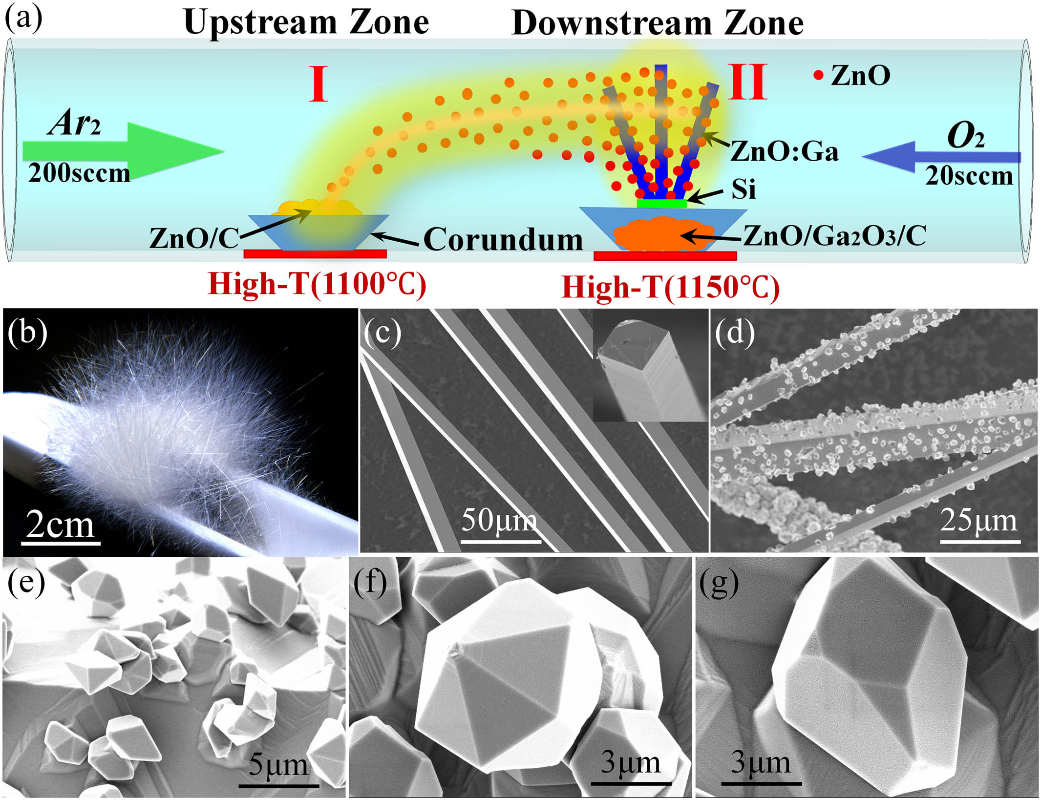
Due to their outstanding surface-to-volume ratio, highly smooth surface, and well-defined crystal boundary, semiconducting micro-/nanocrystals have been used as a pivotal platform to fabricate multifunctional optoelectronic devices, such as superresolution imaging devices, solar concentrators, photodetectors, light-emitting diodes (LEDs), and lasers. In particular, micro-/nanocrystals as key elements can be employed to tailor the fundamental optical and electronic transport properties of integrated hetero-/homostructures. Herein, ZnO microcrystal-decorated pre-synthesized Ga-doped ZnO microwire (ZnO@ZnO:Ga MW) was prepared. The single ZnO@ZnO:Ga MW can be used to construct optically pumped Fabry–Perot (F–P) mode microlasers, with the dominating lasing peaks centered in the violet spectral region. Stabilized exciton-polariton emissions from single ZnO@ZnO:Ga MW-based heterojunction diode can also be realized. The deposited ZnO microcrystals can facilitate the strong coupling of F–P optical modes with excitons, leading to the formation of exciton-polariton features in the ZnO@ZnO:Ga MW. Therefore, the waveguiding lighting behavior and energy-band alignment of ZnO microcrystal-sheathed ZnO:Ga MW radial structures should be extremely attractive for potential applications in semiconducting microstructure-based optoelectronic devices, such as micro-LEDs, laser microcavities, waveguides, and photodetectors.
Photonics Research
2020, 8(2): 02000175

Author Affiliations
Abstract
1 Space Center, Tsinghua University, Beijing 100084, China
2 Beijing National Research Center for Information Science and Technology (BNRist), Beijing 100084, China
We report on a data center network (DCN) architecture based on hybrid optical circuit switching (OCS) and optical burst switching (OBS) interconnect for dynamic DCN connectivity provisioning. With the combination of the centralized and distributed control of the software-defined optical networks, the proposed interconnect can achieve unprecedented flexibility in dealing with both mice and elephant flow in the DCN. Numerical simulation is employed to investigate the performance of the proposed architecture. The results show that the OBS module has preferable performance in dealing with a larger burst packet, and the throughput is constrained by the capacity of the server random access memory module.
060.4510 Optical communications 060.6719 Switching, packet 060.6718 Switching, circuit Chinese Optics Letters
2019, 17(8): 080605
南京信息工程大学物理与光电工程学院, 江苏 南京 210044
基于含石墨烯的双/三层介质结构中的光学色散方程,研究了覆层和基底层材料对石墨烯表面等离子体波横电(TE)模的影响。计算结果表明,近红外波段内,石墨烯表面等离子体波TE模的性质对覆层和基底层介电常数的差值极其敏感。当覆层和基底层介电常数出现微小差异时,TE模可以进行传输。随着两介电常数差值的增大,TE模的有效折射率显著增大,甚至超过覆层折射率,而传播损耗不断减小。对于三层介质结构,相邻两介质分界面间添加单层石墨烯形成了平板波导结构,研究该结构发现,当传导层和基底层介电常数相近时,其夹层的石墨烯对波导TE模的调控尤其显著,这种调控来源于电磁波耦合到石墨烯形成的表面等离子体波TE模。这些结果为设计调制器、检测器和过滤器等石墨烯表面等离子体波导器件提供了理论支持。
表面光学 表面等离子体波 石墨烯 平板波导 横电模 光学学报
2017, 37(11): 1124002
重庆大学教育部三峡库区生态环境重点实验室, 重庆400045
利用荧光检测技术对某垃圾填埋场渗滤液反渗透(RO)膜深度处理时的进水、 出水、 浓缩液、 酸洗液以及酸洗后碱洗液中水溶性有机物(DOM)的组成变化进行了研究。 同步荧光光谱显示, 预处理后的渗滤液膜进水在波长280, 340, 370 nm出现三个较强的荧光峰, 反渗透膜对此有效拦截, 酸洗和碱洗的组合清洗方式有效去除了波长范围在300~420 nm的有机污染物。 三维荧光光谱显示, 进水含有2个类富里酸和3个类蛋白质荧光峰, RO膜出水仅含有2个类蛋白峰, 浓缩液中出现其余3个高强度的荧光峰; 酸洗和碱洗对膜上污染物质分子结构影响显著, 存在着明显的荧光峰位移。 结果表明, RO膜有效拦截了早期渗滤液中的类富里酸, 而对膜的污染物除类富里酸外, 还有类蛋白成分: 主要为低激发类酪氨酸; 为膜污染控制提供了理论支持。
垃圾渗滤液 反渗透 荧光光谱 水溶性有机物 Landfill leachate RO Fluorescence DOM 光谱学与光谱分析
2011, 31(10): 2767
1 浙江大学现代光学仪器国家重点实验室,光及电磁波研究中心,杭州 310027
2 华信邮电咨询设计研究院有限公司,传输设计研究院,传输设计研究三所,杭州 310014
研制了一种新型的超小型电磁驱动微机械可调光衰减器(VOA).该器件采用电磁驱动器转动硅基微镜改变光路实现可调衰减,在结构上采用了全磁性回复,完全摆脱了通常的弹性回复造成的部件疲劳、零点偏移等器件重复性问题.驱动电压为0~5 V,工作范围0~40 dB,插入损耗小于0.8 dB,回波损耗小于-50 dB.器件重要部件采用微细电火花加工(EDM)技术制作,并应用FEA软件进行了结构优化,对衰减响应进行了详尽的理论分析.该VOA设计体积仅为25×10×7mm3,可构成阵列应用于波分复用(WDM/DWDM)系统中各信道的动态信号平衡或网络保护.
光纤通信技术 可调光衰减器(VOA) 微机械(MEMS) 电火花加工(EDM) 密集波分复用(DWDM) Fiber-optic communication technology Variable optical attenuator MEMS EDM DWDM
采用激光全息干涉度量术,在实验室对五种连接体结构各异的上颌双侧游离端部分活动义齿及其相应的牙槽嵴部的受力情况进行了研究.得到了相应的全息干涉国,并对它们进行了定量分析.
全息干涉度量术 牙科义齿


